- Coplanar Band Pass Filter
|
|
Coplanar Lumped Element Band Pass Filter
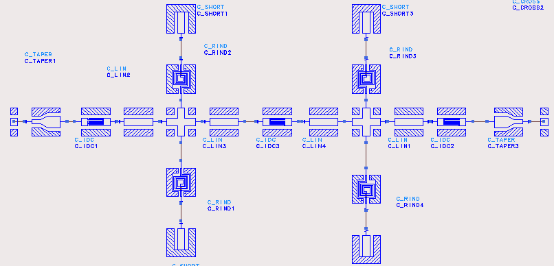
The example documented here is a second order
lumped element bandpass filter for the center frequency of 22
GHz. Figure 9-6 shows the schematic of the filter containing
coplanar interdigital capacitors, coplanar cross junctions,
coplanar shorted ends, coplanar rectangular spiral inductors and
coplanar lines. In this circuit the spiral inductors represents
the parallel resonance circuits, where the parasitics of these
inductors act as capacitances of resonance circuit. The layout of
the circuit is shown in Figure 9-7. As it can be seen in these
figures, two metal layers are used. The interdigital capacitors
are designed in the metal layer 1 because of the low losses of
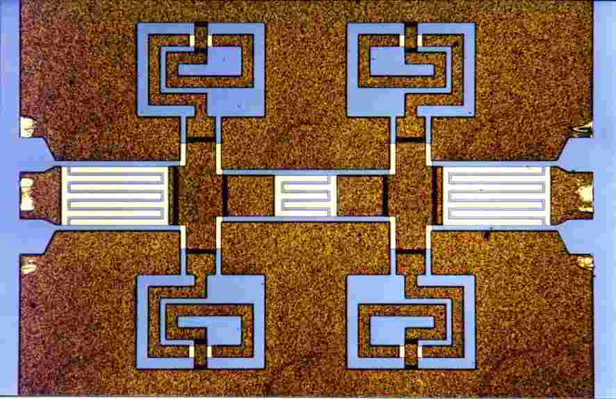
such capacitors. The filter was designed and realized on GaAs.
Figure 9-8 shows a photo of the realized filter. The simulated
and measured scattering parameters of the filter are plotted in
Figure 9-9 showing very good agreement between the measurement
and simulation.
 |
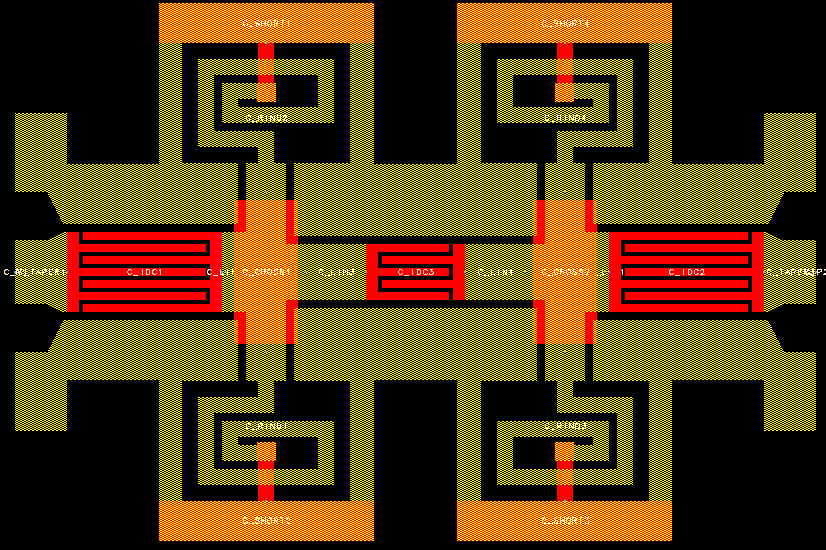 |
| Figure 9-6. Schematic of the Lumped Element Bandpass Filter | Figure 9-7. Layout of the Lumped Element Bandpass Filter |
 |
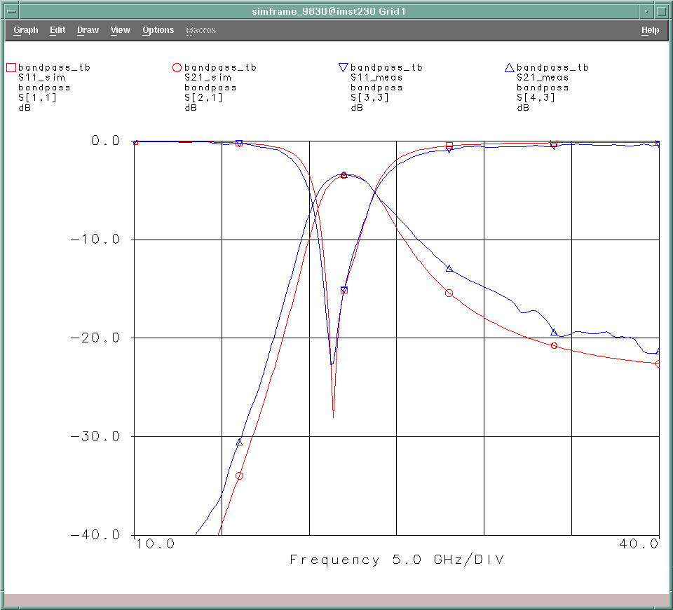 |
| Figure 9-8. Photo of the realized Lumped Element Bandpass Filter on GaAs. | Figure 9-9. Measured and Simulated S-Parameters of the Lumped Element Bandpass Filter |