Coplanar Waveguide versus Microstrip
In the last years, an increase in the design of CPW (CoPlanar Waveguide) circuits on GaAs could be noticed. The main reason for this is the fact that the CPW design technique allows to reduce the circuit size by about 30% and in addition, the expensive backside processing and the difficult via etching in the microstrip case becomes obsolete. In contrast, CPW design results in the disadvantages of slightly higher losses and poor power handling capabilities. Figure 1-1 shows a brief comparison of microstrip and CPW design techniques.
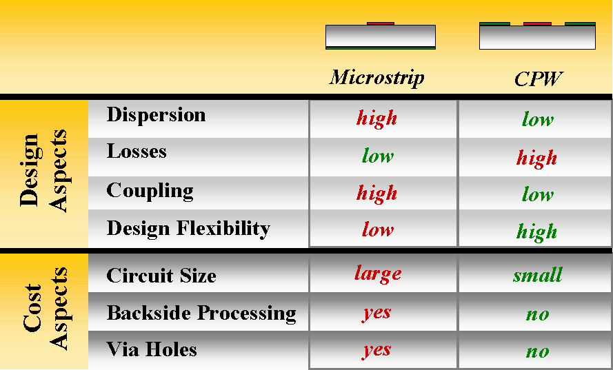
Figure 1-1: Comparison between microstrip and CPW design techniques
Although there are many encouraging activities in CPW design, this technique has not yet achieved the real breakthrough. The main reason for this is the lack of a complete, accurate CAD oriented CPW element library. With COPLAN for Libra such a library is now available in the environment Series IV of HP-EEsof.
At present, there are four possible techniques for the design of coplanar circuits. Figure 1-2 shows the comparison between these techniques due to the cost and time consumption as well as accuracy and validity aspects.
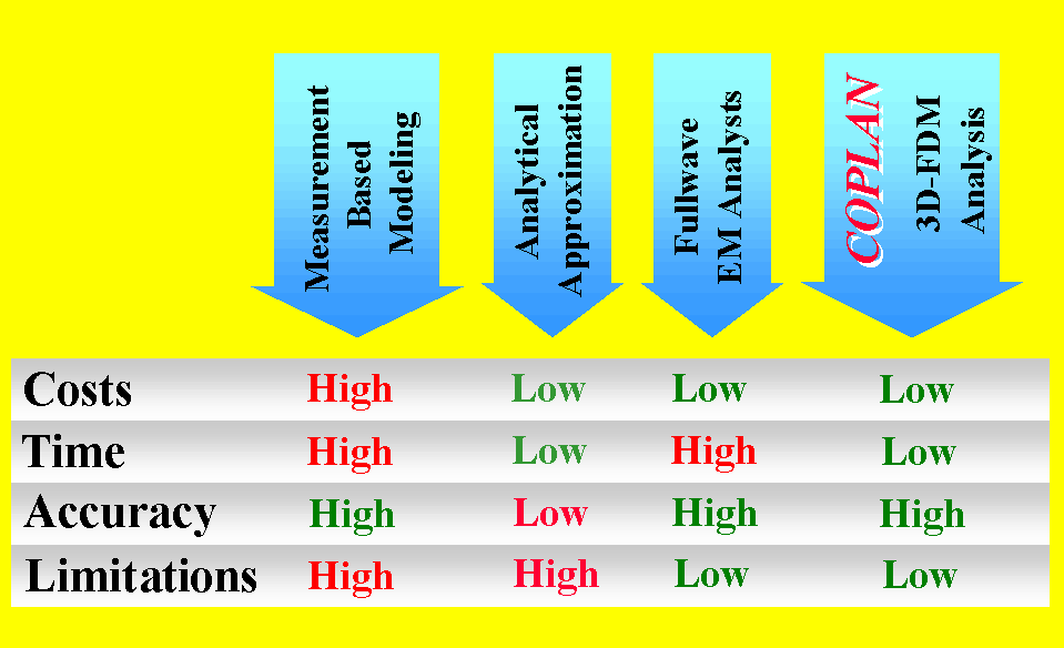
Figure 1-2: Coplanar Design Techniques
By the measurement based modeling, a great number of test structures have to be realized and measured. The measured data are then used for the modeling of these structures. The realization and measurement of test structures take too long and lead to high costs. This technique has the advantage of great accuracy, but this accuracy is limited to certain dimensions and substrate parameters The results are valid only for the measured frequency range.
Another method which is often used for the simulation of CPW-circuits is the use of analytical approximations. However, in spite of microstrip lines, there is only a few number of such approximations for coplanar structures.
An alternative is the use of EM-Field solvers, which overcome the problem of cost and limitation of validity range. But, the use of such tools is very complicated and the simulation time is very large. As a result, the design of large circuits and the optimization of circuit performances are not possible.
Features of COPLAN AT a Glance
COPLAN for Libra enables the designer of coplanar circuits to simulate and optimize the circuit parameters in a relatively short time. There is no limit due to the structure dimensions and the results are very accurate for a wide range of frequencies. Figure 1-3 shows the features of COPLAN for Libra at a glance.
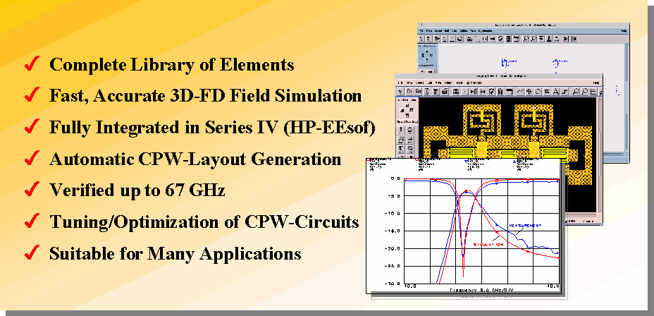
Figure 1-3: Features of COPLAN for Libra at a glance.
The complete spectrum of coplanar elements is implemented. Elements from single and multiple coupled coplanar lines over discontinuities like step, gap and bend up to the three and four port junction elements with and without air-bridges are available. To complete this library, also lumped elements such as rectangular inductors, interdigitated capacitors, MIM capacitors and thin-film-resistors are also included in this library. The schematic circuit entry as well as multi-level layout generation is completely supported besides the accurate simulation of such elements.
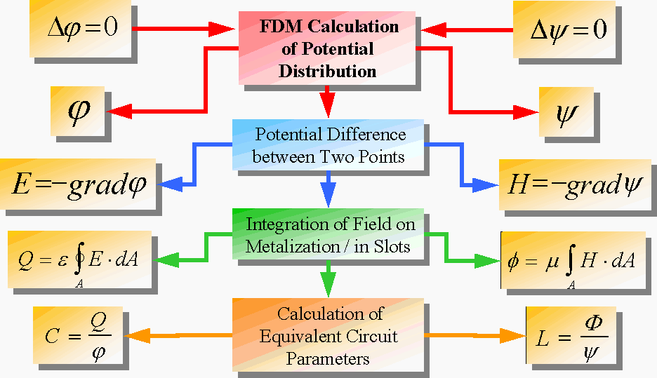
The kernel of this new and state-of-the-art library is based on a field-theoretical modeling of coplanar structures using a sophisticated 3D quasi-static finite difference (Figure 1-4). Such a 3D simulation is necessary since true 3D structures are needed for the air-bridges e.g. Due to the 3D approach, the metallization thickness can be taken into account during the calculations. Three layers of dielectric material are available with arbitrary physical parameters.
|
Figure 1-4: Field Theoretical Modeling of Coplanar Structures used in COPLAN for Libra |
The above mentioned numerical method is applied to each of the elements in such a way, that a parametric description (equivalent circuit) of the elements resulted. Thus, the actual implementation of the numerical calculations allows circuit optimization for instance.
To make the utilization of COPLAN for Libra more efficient, a smart cache memory will speed up optimizations and statistical analysis. The implemented CACHE works as follows: The first numerical analysis of a CPW element will completely go through the algorithms. In the second run, the CACHE management identifies already calculated structures and loads previously calculated results. Therefore optimization of CPW circuits, including numerical CPW elements, becomes possible in a matter of seconds.
As a conclusion it can be said, that the CPW elements within HP-EESOF Series IV can be used similarly to the well known microstrip elements. The complete layout generation of CPW designs is supported up to the level of foundry requirements. Thus, for the first time it becomes possible to accurately design CPW circuits with only little manual effort.