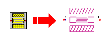
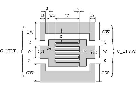
The C_IDC module represents an interdigitated capacitor between center conductor of two coplanar lines. The dimensions of lines are defined using data items addressed by C_ LTYP1 and C_LTYP2 (see C_LINTYP in chapter 4).
L1 and L2 are the length of coplanar lines connected at ports.
A negative value for L1 or L2 can be meaningful during the simulation. In such cases, the automated layout generation works incorrectly and the generated layout has to be edited manually. The minimum values for L1 or L2 depend on the metal layer oversizes in the currently selected foundry. In case of C_LAYER_DEFAULT, L1 and L2 should be greater than or equal to max(|cond_os|, |cond2_os|).
WF is the width of fingers and SF is the distance between the fingers. As shown in the Illustration, the gap at end of fingers is equal to the slots between the fingers.
LF is the length of the fingers (without the slot at the end of fingers). LF should always be greater than SF.
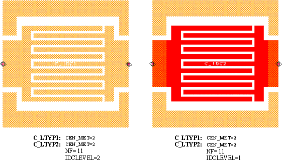
NF is the number of fingers and has to be an integer number. The minimum value for NF is 2. Note that for odd numbers of NF, the number of fingers connected to port one is greater than the number of fingers connected to port 2.
S is the slot between fingers and the ground planes. This parameter influences the parasitic capacitances to the ground (Cp1 and Cp2).
G is the gap between the ground planes and the feed lines connected to the fingers. <0, the automated layout generation works incorrectly and the generated layout has to be edited manually.
WL is the length of feed lines connected to the fingers.
The parameter IDCLEVEL indicates the metal level used for the interdigitated capacitor. The only valid value for this parameter in the DEFAULT foundry is 1 or 2.
If IDCLEVEL and CEN_MET of connected lines are different, an inter metal via is automatically included at the ports. In this case the length of connected lines must at least via_lo in C_LAYER
In the current version, the same C_LTYP is applied at both ports for the simulation (C_LTYP2 = C_LTYP1).
If L1 and L2 in selected C_GRID are not set to -1 (auto sizing), the minimum values for L1 and L2 are:
L1min= max(NF*WF+(NF-1)*SF+2*S+8*DL{C_GRID}, W1+2*S1+2*GW1,W2+2*S2+2*GW2)
L2min= LF+SF+2*WL+2*G+8*DL{C_GRID}
See notations in chapter 4 (Important Note!) for the correct selection of the C_LTYP1 and C_LTYP2.