[to index] [close window]

Resistive Loaded Transmission Line C_TFG

Symbol :

Illustration :

Parameters :

L = Total length of the resistor
C_LTYPR = ID of coplanar transmission line applied at resistive section
C_LTYP1 = ID of coplanar transmission line applied at port 1
C_LTYP2 = ID of coplanar transmission line applied at port 2
RES_IDX = Index to sheet resistivity (ohm/square) definition in currently selected foundry (res_rs)
C_SUB = ID of coplanar substrate definition
C_GRID = ID of simulation control data
TEMP = ID of element temperature definition used for noise computation

Notes/Equations/References :

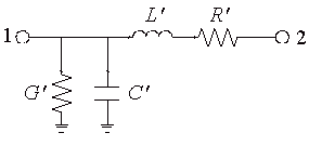
  1. The C_TFG module is introduced to have a resistive connection between center conductor and ground planes (resistor to the ground).

  2. The width of resistor and its distance to the ground are given in a line type addressed by C_LTYPR.

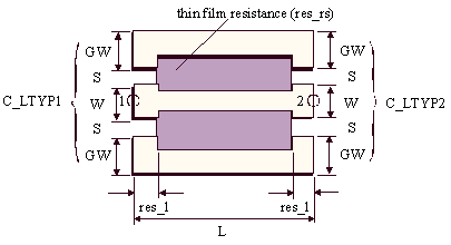
  3. Presently, the C_TFR module is not able to calculate the steps which are made if different line types are used for C_LTYP1, C_LTYP1 and C_LTYPR. Therefore, if a step configuration is used for layout reasons, the effect of such discontinuities are not taken into account during the simulation.

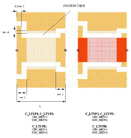
  4. The parameter RES_IDX indicates the index of used resistive layer in the selected foundry. In case of DEFAULT foundry, RES_IDX is always 1.

  5. The effective length of the resistive section is given by L-2*res_l. L must be greater than 2*res_l.

  6. CEN_MET and GND_MET in C_LTYP1 and C_LTYP2 must have the same value. These values are also used for the resistive section (see Layout).

  7. The Parameter CEN_MET and GND_MET in C_LTYPR are ignored.

  8. If L1 in selected C_GRID are not set to -1 (auto sizing), the minimum value for L1 is:

    L1min=max( W1+2*S1+2*GW1, W2+2*S2+2*GW2,WR+2*SR+2*GWR)

  9. See notations in chapter 4 (Important Note!) for the correct selection of the C_LTYP1, C_LTYP2 and C_LTYPR.

Equivalent Circuit :

For the modeling of the C_TFG element, a distributive equivalent circuit is used and the model parameter are derived from quasi-static FD-calculations. since traveling wave effects are considered, there is no limitation due to the length of resistor. The connected lines at ports are modeled as C_LIN elements and are represented by their characteristic impedance ZL and phase constant b.

Layout :

  1. Depending on the metal level of coplanar lines applied to the ports (C_LTYP1 and C_LTYP2), there are different types of resistors.

  2. If the parameter GW_DEF in C_PROCES is set to a positive non-zero value, this value is used as ground width for layout generation.


[to index] [close window]