| Theoretical Background | ||
The kernel of the simulation software is a field-theoretical modeling of elements in conjunction with the so called quasi-static Finite Difference Method (FDM) [2.1, 2.2]. An overview of the applied numerical method for the simulation of coplanar structures is shown in Figure 2-1.
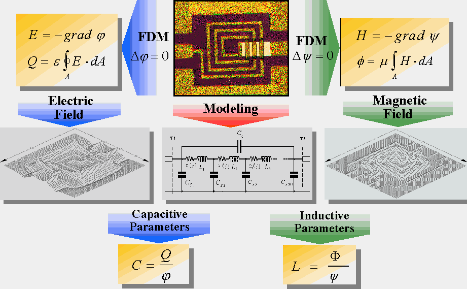 |
| Figure 2-1: Field-theoretical modeling of coplanar structures used in COPLAN for Libra |
The first modeling step is the chose of a suitable broadband equivalent circuit which is able to represent the physical characteristics of the structure in a wide frequency range. The model parameters are then determined by the calculation of the field distributions. For this, the structure is surrounded by a box of electric and magnetic walls and the box space is divided into elementary cells using a grid (discretization). The solution of the Laplace´s differential equation for all grid points leads to the electrical field distribution inside the box as well as the charge distribution on the metalization. This physical quantities are used together with the selected equivalent circuit in order to determine the capacitive model parameters.
In a similar way, the magnetic field distribution as well as the surface current distribution are calculated by solving the Laplace´s differential equation for the scalar magnetic potential. The inductive and resistive model parameters are then derived from the magnetic flux in slots and surface current on conductors.
The choice of the equivalent circuit is an important step by the modeling. In order to take the high frequency characteristics of coplanar structures into account, a broadband equivalent circuit is necessary. This is only possible if all parasitic effects are considered in the selected model. The selection of such broadband models is demonstrated in Figure 2-2 for more complex structures like spiral inductors. For a large number of turns, the use of a simple equivalent circuit (consisting of a single pi-network) would lead to the limitation of the validity range. Therefore, a more accurate equivalent circuit is applied, where each turn of the inductor is represented by a pi-network. The electrical coupling between the turns (partially caused by the air bridge) is considered by the capacitance Cg between the ports.
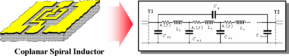
Figure 2-2: Broad band modeling of a coplanar spiral inductor
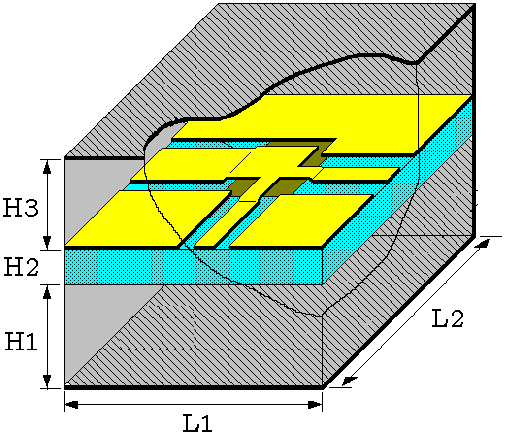
For the calculation of the electric and magnetic field distribution, the coplanar structure is surrounded by a shield of electric and magnetic walls (Figure 2-3A). Magnetic walls are assumed at ports, where the feed lines intersect the shielding. The distance between the magnetic walls and reference planes of the structure (length of feed lines at ports) effects the accuracy of the results and should therefore be chosen properly. The distance of electric walls from the structure should also be large enough in order to keep their effects as small as possible. An exception is the case where the effects of packaging should be taken into account. The dielectric constant of the area above and below the structure can differ from the value for air (er=1). In this way, multilayer substrate configurations can be calculated.
|
| Figure 2-3: A) Shielded multi-layered substrate used for the field calculation. |
The volume inside the shielding box is now divided into elementary cells using a 3-dimensional non-equidistant grid (Figure 2-3B). The discretization is done automatically in such a way that the area near the metalization surface is discretized much finer than the space above and below the substrate surface. The reason is the fact that the field is more concentrated near by the metalization surface. For the implementation of this method in a CAD-tool and in order to speed up the calculation , an efficient and automatic discretization is implemented.
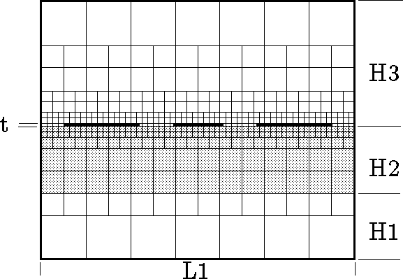 |
| Figure 2-3: B)Non-equidistant discretization as used in Coplan for Libra. |
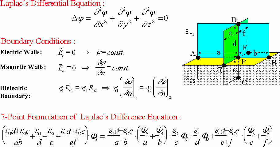
For the calculation of electric and magnetic potential distribution inside the shielded box, the Laplace´s differential equation is solved. A 7-point formulation is derived from Laplace´s difference equation using the corresponding boundary conditions. The possible boundaries are: electric walls, magnetic walls and dielectric boundary. The 7-point formulation expresses the electrical potential at any grid point P inside the box as a function of potentials at 6 neighboring points and their distances to the point P (Figure 2-4).
|
Figure 2-4. The 7-Point Formulation of Laplace´s Equation
For the numerical determination of the potential distribution inside the box, the iterative method of "Over Relaxation" (OR) is used. At first, an initial potential is assumed in all points. The potential at any point of grid is then corrected using the mentioned 7-point formulation. This procedure is repeated as long as the mean error between the corrected potential and the previously calculated potential for all points of grid is less than a defined iteration error. Using the potential difference between two points in x, y or z-direction, the electric and magnetic field distribution can be determined for all points inside the box.
From the electrical field inside the shield, the total charge on the metalization Qtotal and the charge per unit length on the connecting transmission lines Q' are calculated. Since the potential difference between the inner conductor and the ground plane is known to be V, the capacitance(s) Ceq associated to a given structure is then calculated as the difference between the total charge Qtotal and the charge per unit length Q' of the virtual transmission lines connected at ports:
Ceq=(Qtotal-l.Q')
where l is defined as the virtual distance between the back-transformed reference planes of the discontinuity and the magnetic walls.
The calculation of capacitive model parameters is demonstrated here in case of an interdigitated capacitor. The procedure is shown in Figure 2-5. Two different potential configurations are used for the calculation of shunt capacitances Cp1 and Cp2 as well as the couple capacitance Cg. By the so called even mode simulation, the center lines and the fingers of the capacitor are set on the same potential of 1Volt whereas the ground planes are set to zero Volt. The solution of the Laplace´s equation leads to the field distribution on the metalization. The shunt capacitances Cp1 and Cp2 are calculated from the charge distribution on the conductors.
 |
| Figure 2-5: Electric potential configurations for the calculation of the equivalent capacitances of an interdigitated capacitor |
For the calculation of the coupling capacitance Cg, a so called odd mode simulation is necessary. In this case, the fingers of the capacitor are set to opposite potentials of 1Volt and -1Volt. The ground planes are set to zero Volt. After the calculation of the potential distribution, the charges on conductors are used for the determination of the capacitance Cg.
To determine the equivalent inductances, NAGHED introduced in [2.4] the following procedure. First of all, a given geometry must be inverted, that means, the slots become metal and vice versa (Figure 2-6). Because of the fact that the slots in coplanar structures act as the magnetic wall, constant magnetic scalar potentials are assumed in the area of slots between the metalization. After that, the magnetic scalar potential can be calculated similar to the electrical potential.
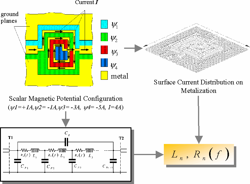 |
| Figure 2-6: Magnetic potential configuration for the calculation of the equivalent inductances of a spiral inductor |
Once the magnetic field in the coplanar slots is known, the integral over the slot surface leads to the magnetic flux and the surface current distribution, which is used for the calculation of the total flux of the structure. Since the magnetic potential difference in slots is known to be y, the equivalent inductance Leq is then calculated from the difference between the total flux Øtotal and the flux per unit length Ø' multiplied by the geometrical length l of the virtual coplanar lines at ports:
Leq=( Øtotal-l.Ø') / y
where l is defined as the virtual distance between the back-transformed reference planes of the discontinuity and the magnetic walls.
Under assumption of low losses, equivalent resistances and conductances are used for the modeling of metallic and dielectric losses respectively. The surface current distribution calculated form the magnetic field is utilized for the determination of the metallic losses. DC resistance as well as frequency dependent RF-losses due to the skin effect are taken into account.
From the comparison of the capacitance with and without the dielectric substrate the electrical field energy inside the substrate can be obtained. Using this quantity and using the loss tangent of the substrate, dielectric losses are determined.
Convergence, Stability and Numerical Accuracy
The integration of the FDM into CAD software and the intensively use of these programs makes it necessary to investigate some properties of the simulator, like the numerical stability, accuracy setting and convergence behavior. On one hand this will help the user to minimize computation time and to optimize the numerical results. On the other hand the series of simulations will be used for the automation of some model parameters, like the discretization or the iteration boundary. The following calculations were made for a GaAs substrate (er=12.9) with a thickness of 500mm. For explaining the investigations, the coplanar transmission line model was used, which has the advantage of a simple geometry.
At first the influence of two numerical parameters, the grid size DL and the iteration error BOUND on accuracy of the simulation results for a coplanar line are investigated (see C_GRID). A coplanar line configuration with the following parameters has been chosen to ensure, that the grid crossings are always on the edges of the metallization: Substrate height h=500mm, er=12.9, w=50mm, s=40mm with a metalization of gold and a thickness of t=3mm. Figure 2-7 depicts the calculation of the line characteristics and its relative error as a function of grid size DL and iteration error BOUND. The relative error decreases with smaller size of DL, whereas the iteration error BOUND has no significant effect as long as the grid size is not too small (here DL³ 5 mm). For very fine grid (DL£ 2.5) there is an influence of the iteration error on results.
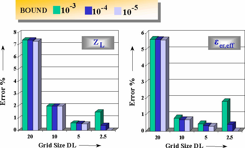 |
| Figure 2-7: Influence of the grid size DL (in mm) and the iteration error BOUND on simulation accuracy by the calculation of coplanar line characteristics |
The two following statements describe the relation of the discretization size and the iteration error in a basic formulation:
The calculations of very small and wide coplanar lines have been evaluated to achieve common statements for the convergence behavior of the simulator. One can obtain a relative error, which is always lower than 1%, if the iteration error is 10-3 and the cell size DL is lower than the smallest line dimension divided by 4. For a fast simulation run or a big number of calculations (e.g. during an optimization), a coarse discretization (the smallest line dimension divided by 2) is already sufficient.
Further convergence investigations proof, that even for very fine grid (smallest line dimension divided by 64) and small iteration error (10-6) the simulator is numerically stable. Figure 2-8 shows the effect of grid size by the calculation of a microstrip line impedance. The calculation time rises from some milliseconds up to 15 minutes (on a workstation HP9000, 160MHz, PA 8000).
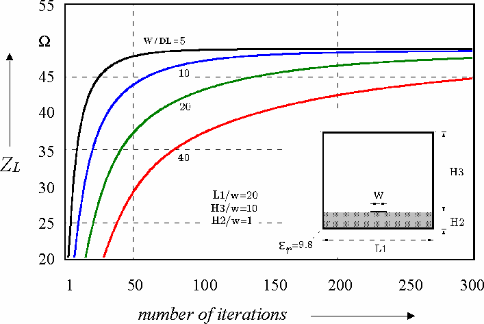
Figure 2-8. The effect of grid size DL on numerical convergence
The simulation time depends on a series of different aspects such as chosen numerical parameters (box sizes, mesh size, iteration error, etc.), structure dimensions or hardware performances. The investigations which are documented here should be a guiding value. The used hardware is on a workstation HP9000, 160MHz, PA 8000. The required simulation time for CPW-elements is shown in Figure 2-9. The numerical parameter are chosen for an optimum combination of time and accuracy.
 |
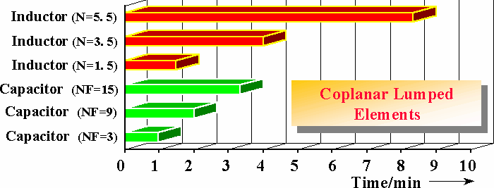 |
| Figure 2-9. Simulation Time for Coplanar Elements (on a workstation HP9000, 160MHz, PA 8000) |
For single coplanar line (C_LIN), metal-via (C_METVIA), coplanar MIM-capacitors (C_MIM, C_CAPLIN) and thin film resistors (C_TFR, C_TFG), the simulation time is usually less than 1 second. For simple discontinuities, a simulation time between 10 and 30 seconds is needed, whereas the calculation of junctions takes about 1 to 2 minutes. This is because of the large number of equivalent circuit parameters and slow convergence of the numerical calculation as a result of the grater number of magnetic walls at ports.
In case of more complicated structures like interdigitated capacitors and spiral inductors, the simulation time depends strongly on the structure dimensions like number of fingers or turns. In such cases, the simulation can take between 1 and 10 minuets.
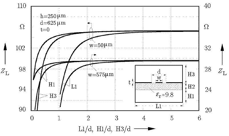
The accuracy of the applied method depends also on the size of shielding box. The width L1 and the depth L2 of the shielding box can be specified using the data item C_GRID. The distance to the cover shield H3 as well as the distance to the bottom shield H1 have to be selected in C_SUB . The influences of electric shielding walls (parameter L1, H1, H3) are investigated for two different CPW lines with the same total width d (d=W+2S) and different center line widths W (50 mm and 575 mm). The results are plotted in Figure 2-10. The width of the box L1 (distance to the lateral electrical walls) is the critical parameter specially in case of eeff calculations, whereas the distance to the upper and lower cover has a marginal effect. It is necessary to select L1 > 5d in order to keep the influence of the lateral shielding walls as small as possible. For H1 and H3, a value of 2d is mostly sufficient.
 |
 |
Figure 2-10.Dependence of the line impedance ZL and effective permittivity eeff of coplanar waveguide on shielding sizes (d=w+2s) |
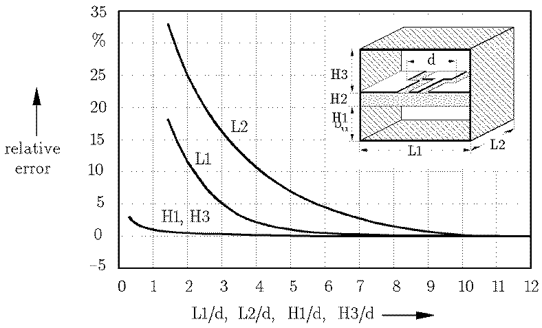
The effects of shielding on the calculated model parameters for 3-dimensional structures (discontinuities and lumped elements) are investigated in case of a coplanar step. In Figure 2-11, the relative error by the calculation of the step capacitance (upper diagram) and step inductance (lower diagram) are plotted against the shielding dimensions. The parameter L2 which indicates the distance to the magnetic walls must be 10d (d=max(W1+2S1, W2+2S2)) in order to neglect the effects of magnetic walls.
 |
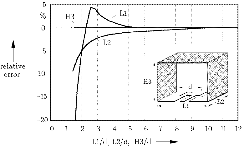 |
Figure 2-11.Dependence of the calculated model parameters of a coplanar step on shielding sizes (d=w2+2s2). |